More idea for Flower ProtoBoard ??
January 12, 2019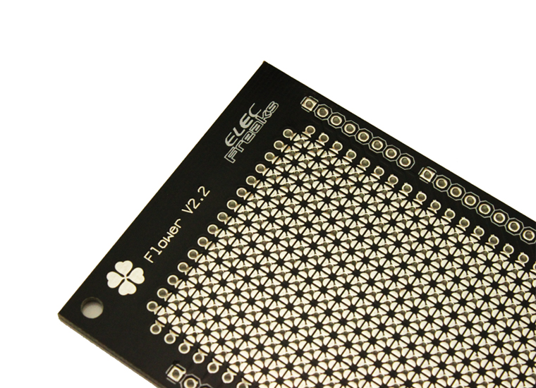
ProtoBoard Revolution – Flower ProtoBoard
January 12, 2019Since we released the flower protoboard, we have received a lot of suggestions. Thank you for all you have done for us. In order to give you a more in-depth understanding of our Flower serials, we will give you a brief description of the evolution of the Flower family history,which I hope will give you more ideas and imagination. We are always thinking about what kind of protoboard is the most convenient for us.What can we improve the traditional protoboard? We found that it was hard to use point-to-point wiring on the traditional protoboard. It need lots of practice and solder, and most of them were wasted. Besides,it was hard to solder SMD devices on traditional protoboard. However, SMD devices are very popular nowadays. Therefore, we aimed at such applications and put forward a new protoboard requirements.
- At first, it must be compatible with the traditional protoboard, Including all the features and benefits of traditional protoboard.
- Secondly, it must beable to solder some SMD devices.
- Finally, It must fit for beginners, easy enough to solder and wire. Maximize saving solder. We think that is flower protoboard’s biggest innovation for protoboard.
Version 1
In accordance with this requirement, we have produced the first protoboard. As the following picture shows that we tried two different pads, one is the flower-shaped pad, the other is a square pad.
The flower protoboard has been largely achieved our requirements, you can solder SMD .components easily.
However point-to-point wiring is not optimism, it is still need a lot of solder.
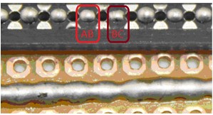
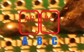
As traditional bread board, AB solder joint is destroyed when you solder BC joint( between point B and point C). You need to solder AB joint again, and it may destroy the another joint at this time. Solder again and again, not only troublesome, but also a waste of solder.
So this is our first failed version. In our analysis, maybe the reason of wiring difficult is the long distance between the pad. So we decided to make improvements in the next version.
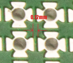
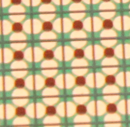
This version, we shortened the distance between the pads, increased pad area of the petals, and eliminated the square pad.
It easier to wiring between pads and solder SMD devices. But there is still a fatal problem. The solder often flow to other ‘petals’ when you wiring. Finally, becoming very thick solder. It did not achieve the purpose of saving solder.
So we decided to continue the development of the next version. After analysis,We found that the reason of solder flow to orther ‘petals’ is one more cirque in the middle of flower pad. The cirque is indeed a seemingly insignificant factor, but it cause the failure of the PCB.
Version 3
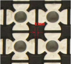
We learned the lessons of the version 1 and version 2 failure. Maximum reduce the distance between the pad, remove the center cirque. And test 2 layers PCB and single layer PCB. We finally get a satisfactory results.
Version 4
Flower v2.2 protoboard is based on version 2 and learned the lessons of previous 3 versions. It has been fully able to meet our original intention to develop new protoboard.
As the following picture shouwn that it just need a very small amount of solder when use point-to-point wiring. AB and BC joints are independent of each other. So, you can avoid destroying AB joint when solder Bcjoint. This obviously makes the wiring easier.
his time we produced 20 pcs Flower Mega ProtoBoard for sample.
So we encourage guys who are experienced engineer or with extensive welding experience, and willing to write a test comment for us. Welcome to request for free product samples.
Please send you request to : [email protected]
Request Sample Format:
—· Willing to write a test report or comment for flower ProtoBoard. You can post on yourself Blog or electronics enthusiast Form, please send the post link to us. Of course you also could feedback your report to us or within the post. Any suggestion to improve the Flower ProtoBoard Series is Welcome.
—· Contact person and phone number
—· Shipping address


